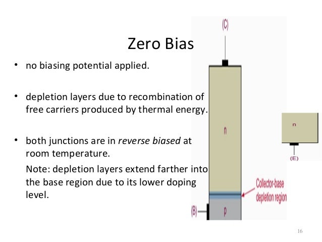
Definition Of Zero Bias

Pn Junction Diode And Diode Characteristics

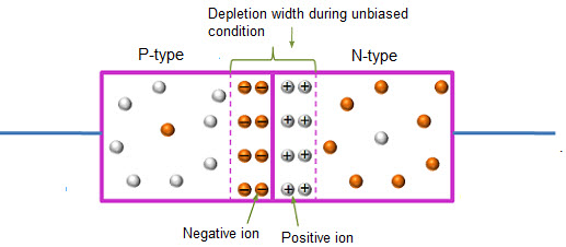
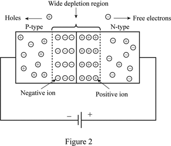
Zero Bias Pn Junction

Diode Junction Capacitance Transition Capacitance And Diffusion Capacitance
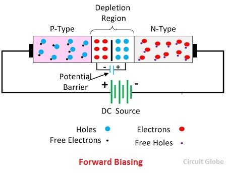
Difference Between Forward Reverse Biasing With Comparison Chart Circuit Globe
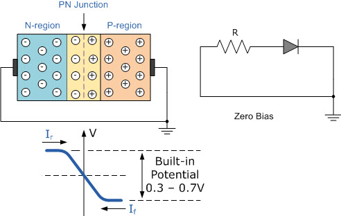
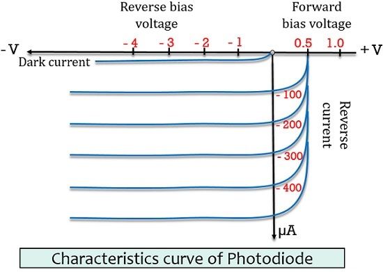
Vi Characteristics Of Pn Junction Diode In 3 Biasing Modes

P N Junction Diode Baising And Its Vi Characteristics Electronics Basics Diode Junction
Find out information about zero bias.
Definition of zero bias. It often manifests in cases where decision makers address problems concerning health safety and the environment. Zero risk bias is an irrational logic that we apply when making a choice leading our brains to prefer an option that totally eliminates any risk over options that could in fact eliminate more risks and could end up with better results. The p n junction in which no external voltage is applied is called zero bias p n junction. Choices with zero risk offer certainty which the brain seeks to maximize in order to reduce cognitive strain.
The condition in which the control grid and cathode of an electron tube are at the same direct current voltage. So when presented with two options we will go with the one that eliminates a small risk completely rather than. Zero risk bias refers to our tendency to opt for complete risk elimination sometimes over an alternative that actually offers greater overall predicted outcomes. Zero bias p n junction is also called as unbiased p n junction.
The zero bias transform is a transform from one probability distribution to another. Zero risk bias is a tendency to prefer the complete elimination of a risk in a sub part even when alternative options produce a greater overall reduction in risk. Mcgraw hill dictionary of scientific.

Chapter 5 Solid State Diodes And Diode Characteristics Analog Devices Wiki
Latest Topic 4 Bipolar Junction Transistors
P N Junction Diode Baising And Its Vi Characteristics
Is A Zero Risk Bias Impairing Your Crisis Response Psychology Today

Semiconductor Pn Junction Diode Working P N Diode Vi Characteristics Semiconductor Diode Depletion Region

Neural Network Bias Bias Neuron Overfitting And Underfitting Missinglink Ai

Sensitivity Drift An Overview Sciencedirect Topics

Semiconductor Electronics Diode Construction And Operation Wikibooks Open Books For An Open World

Body Bias What It Is And Why You Should Care
Bias Variance Decomposition Mlxtend
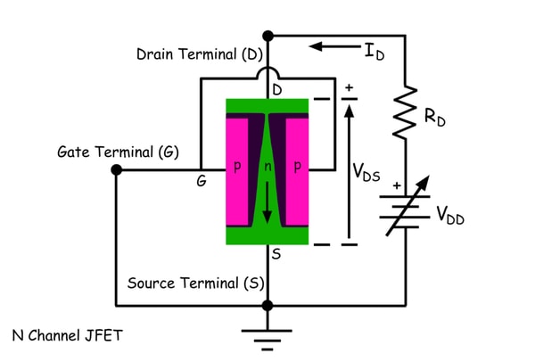
Biasing Of Junction Field Effect Transistor Or Biasing Of Jfet Electrical4u

Schottky Diode Or Schottky Barrier Semiconductor Diode
Definition Of Junction Capacitance Chegg Com